ZG4N60N,,,,,.,,.ZG4N60 is an N-channel enhancement mode MOSFET, which is produced usingZhongxinMicro-electronics's proprietary. The self-aligned planar process and improved terminal technology reduce the conduction loss, improve switching performance and enhance the avalanche energy. The transistor can be used in various power switching circuit for higher efficiency and system miniaturization. MAIN CHARACTERISTICS VDSS600V ID4.0ARDS(ON)2.0ΩCrss8pF ABSOLUTE MAXIMUM RATINGS (Tc=25ºC) ParameterSymbolValueUnit-Drain-Source VoltageVDSS600VContinues Drain CurrentIDTc=25ºC4*ATc=100ºC2.5*( 1)Plused Drain Current (note 1)IDM16AGate-to-Source VoltageVGS±30V( 2)Single Pulsed Avalanche Energy (note 2)EAS218mJ( 1)Avalanche Current (note 1)IAR4.0A( 1)Repetitive Avalanche Energy (note 1)EAR10mJ( 3)Peak Diode Recovery (note 3)dv/dt4.5V/nsPower DissipationPDTc=25ºCTO-251/TO-25251WTO-220/TO-262100TO-220F33Power Dissipation Derating FactorPD(DF)Above 25ºCTO-251/TO-2520.39W/ºCTO-220/TO-2620.8TO-220F0.26 Operating and Storage Temperature RangeTJ,TSTG150,-55~+150ºCMaximum Temperature for SolderingTL300ºC THERMAL CHARACTERIASTIC ParameterSymbolMaxUnitThermal Resistance,Junction to CaseRth(j-c)TO-251/TO-2522.5WTO-220/TO-2621.25TO-220F3.79Thermal Resistance,Junction to AmbientRth(j-A)TO-251/TO-25283W/ºCTO-220/TO-26262.5TO-220F62.5* * Drain current limited by maximum junction temperature ELECTRICAL CHARACTERISTICS Off-CharacteristicsParameterSymbolTests ConditionsMinTypeMaxUnit-Drain-Source Breakdown VoltageBVDSSID=250μA, VGS=0V600--VBreakdown Voltage Temperature Coefficient△BVDSS/△TJID=250μA, referenced to 25ºC-0.7-V/ºC Zero Gate Voltage Drain CurrentIDSSVDS=600V,VGS=0V, TC=25ºC--1μAVDS=480V, TC=125ºC--10Gate-body leakage current, forwardIGSSFVDS=0V, VGS =30V--100nAGate-body leakage current, reverseIGSSRVDS=0V, VGS = -30V---100nA On-CharacteristicsParameterSymbolTests ConditionsMinTypeMaxUnitGate Threshold VoltageVGS(th)VDS = VGS , ID=250μA2.0-4.0VStatic Drain-Source On-ResistanceRDS(ON)VGS =10V , ID=2.0A-2.02.5ΩForward TransconductancegfsVDS = 40V, ID=2.0A (note4)-4.0-S Dynamic CharacteristicsParameterSymbolTests ConditionsMinTypeMaxUnitInput capacitanceCissVDS=25V, VGS =0V, f=1.0MHZ-510660pFOutput capacitanceCoss-5470pFReverse transfer capacitanceCrss-810pF Switching CharacteristicsParameterSymbolTests ConditionsMinTypeMaxUnitTurn-On delay timetd(on)VDD=300V, ID=4A, RG=25Ω(note 4,5)-1642nsTurn-On rise timetr-48112nsTurn-Off delay timetd(off)-48105nsTurn-Off Fall timetf-3886nsTotal Gate ChargeQgVDS =480V , ID=4A, VGS =10V (note 4,5)-1520nC-Gate-Source chargeQgs-2.8-nC-Gate-Drain chargeQgd-6.8-nC - Drain-Source Diode Characteristics and Maximum RatingsParameterSymbolTests ConditionsMinTypeMaxUnitMaximum Continuous Drain-Source Diode Forward CurrentIS--4AMaximum Pulsed Drain-Source Diode Forward CurrentISM--16ADrain-Source Diode Forward VoltageVSDVGS=0V, IS=4A--1.4VReverse recovery timetrrVGS=0V, IS=4AdIF/dt=100A/μs (note 4)-320-nsReverse recovery chargeQrr-2.4-μC :1:2:L=25mH, IAS=4A, VDD=50V, RG=25 Ω, TJ=25ºC3:ISD ≤4A, di/dt ≤300A/μs, VDD≤BVDSS, TJ=25ºC4::≤300μs,≤2%5:Notes:1:Pulse width limited by maximum junction temperature2:L=25mH, IAS=4A, VDD=50V, RG=25Ω, Starting TJ=25ºC3:ISD ≤4A, di/dt ≤300A/μs, VDD≤BVDSS, Starting TJ=25ºC4:Pulse Test: Pulse Width ≤300μs, Duty Cycle≤2%5:Essentially independent of operating temperature ELECTRICAL CHARACTERISTICS (curves) 1. 2. Fig. 1 On-State Characteristics Fig. 2 Transfer Characteristics 3. 4. Fig. 3 Breakdown Voltage Variation vs Temperature Fig. 4 On-Resistance Variation vs Temperature 5. 6. Fig. 5 Capacitance Characteristics Fig. 6 Gate Charge Characteristics 7. 8. Fig. 7 Maximum Safe Operating Area Fig. 8 Maximum Drain Current vs Case Temperature9. (TO-251/TO-252) Fig. 9 Transient Thermal Response Curve (TO-251/TO-252) 10. (TO-220/TO-262)Fig. 10 Transient Thermal Response Curve(TO-220/TO-262)11. (TO-220F)Fig. 11 Transient Thermal Response Curve(TO-220F) TEST CIRCUITS AND WAVEFORMS 12. Fig.12 Resistive Switching Test Circuit & Waveforms13. Fig.13 Gate Charge Test Circuit & Waveform14. Fig.14 Unclamped Inductive Switching Test Circuit & Waveforms TPACKAGE MECHANICAL DATA TO-251 DIMMILLIMETERSDIMMILLIMETERS A2.2±0.5H1.8±0.5 B5.2±0.25I0.8±0.05 C5.3±0.25J0.508±0.015 D4.5±0.5K2.3±0.25 E6.3±0.25L0.5±0.1 F2.3±0.05M0.508±0.015 G0.6±0.05N7.5±0.5 TO-252 DIMMILLIMETERSDIMMILLIMETERSA2.2±0.5
Quality 4n60 Mosfet Original Quality Transistors To220/220f/252/263 products, provide good price 4n60 Mosfet Original Quality Transistors To220/220f/252/263 from Jiangsu Zhongxin Semiconductor Co., Ltd..
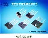
Larger photo of 4n60 Mosfet Original Quality Transistors To220/220f/252/263
Related products about 4n60 Mosfet Original Quality Transistors To220/220f/252/263
-
 Waste Tyre Plastic Recycling Machinery Machine Tire Crusher Production Line Rubber Crumb Grinding Machine Equipment Tire Shredder
-
 Stretch Plastic Blowing Pet Bottle Making Blow Molding Machine Bottles Stretch Automatic Pet Bottle Blowing Machine
-
 Waste Plastic Pet Bottle, Water Bottle Flake, PP/HDPE/LDPE PE Film Jumbo Woven Bags Plastic Crusher Machine, Plastic Crushing Washing Recycling Machine
-
 Type 2 Wall-Mounted Electric Car Charging Station 7kw /11 Kwelectric Vehicle Charging Station Home Wallbox AC EV Charger Single Phase or 3three Phase
-
 G-View G12W Wholesale Auto Car LED Headlight Bulb High Power H13 H11 9005 H7 H4 Car LED Headlights LED Car Lights
-
 New Design Porcelain Round Plates Dinner Set for Wedding and Banquet
-
 China 2023 New Design Super Soft 100% Polyester Microfiber Knitted Oversized Decoration Hoodie Blanket
-
 Handmade Art Creative Materials Thickened White Paper Cup DIY Disposable Handmade Colored Paper Cup


